This blog wish to help anybody that wants to learn the magic world of Software Defined Radios. I will be using what is defined as bladeRF - the USB 3.0 Superspeed Software Defined Radio, AN OPEN EDUCATION since the spirit of the project is in line with my wishes
What will follow are notes and details that I could not esly find in the reference website but have discovered on my own
For some of us what I will be writing is obvious, for some others it is not. You may find some interesting facts here. The key point is what platform you are running on, mine is Kubuntu 12.04
You MUST accept default location for quartus 12, mine ended up being /home/damiano/altera/12.1sp1 choosing a different one will give you troubles
Finally it is clear what happensThe git project is an incomplete quartus project, to be complete you MUST use the build script, not the tcl script, the shell script since that one copies pieces and fix things to make a full working project under the work directory
What you have to open is bladeRF/hdl/quartus/work/bladerf.qpf
Get the bladeF project using git clone https://github.com/Nuand/bladeRF.git
The README in the quartus directory of bladeRF simply says to use build_bladerf.sh but this does not work if you do not have a setup for quartus.
The easiest way to do it is to execute a script that provides an environment preset, you con find it into
~/altera/12.1sp1/nios2eds$ ./nios2_command_shell.sh
Once you are in the quartus envoronment shell you change directory to the bladeRF/quartus and execute the script
~/work/altera/bladeRF/hdl/quartus$ ./build_bladerf.sh -r hosted -s 115
You can then open the project using
cd ~/altera/12.1sp1/quartus/bin; ./quartus bladeRF/hdl/quartus/work/bladerf.qpf
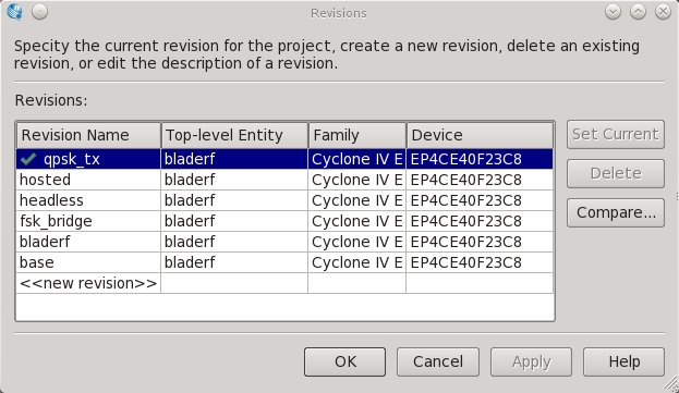
You should end up with a revisions windows that looks like this one 
One interesting bit is the creation of the hex file holding the proram
Post-processing to create mem_init/nios_system_onchip_memory2_0.hex...
bash -c 'elf2hex lms_spi_controller.elf 0x00004000 0x00007fff --width=32 \
                --little-endian-mem --create-lanes=0  mem_init/nios_system_onchip_memory2_0.hex'
The very first step is to define the FPGA chip pin connections, you could do it manually or you can use the ones that come with the bladeRF GIT project. However, with quartus II version 13.1 it is advisable to name pins without the array subscript, this is what quartus says, ate least for pin that are input and output (not bidirectional, simply some are input, some are aoutput)
I have done an export of bladeRF pin definition that you may wish to import for your use, bear in mind that Quartus is quite happy to allocate a new pin that was unused for a new label and it is therefore strongly advisable to check the compiled project to see if all pins are where thay are supposed to be.
If any of you wish to plan with the FPGA I really suggest to buy the io expansion board.
It is worth the money since it allows you to have much more feedback on what happens within the FPGA.
The original schematics of GPIO expansion board has odd and even pin number swapped.

Using part of pins to assing output
exp_gpio <= ( 8 => lms_rx_clock_out, others => 'Z' );to read input
another_sig <= exp_gpio(9);
register for DC offset engidea: btw there is a register, 0x5a iirc, that improves dc offset. you might want to try that
One of the first thing that are needed when dealing with FPGA is having a clock source. BladeRF has a clock source named c4_clk that enters the FPGA on pin A11. The clock source is derived from the Si5338 and I can confirm that it is active even if no programming is done to the chip.
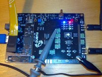
The first thing you may wish to do is to output the clock to the expansion board, just to confirm that the whole Quartus,programmer, board are ok. To do this you just need to create a derivative megafunction of ALTPLL called clock_pll and use the following snippet of verilog
module blade1_led(
	exp_gpio_19,
	exp_gpio_8,
	exp_gpio_24,
	exp_gpio_23,
	exp_gpio_29,
	c4_clock
);


input wire	c4_clock;
input wire	exp_gpio_19;
output wire	exp_gpio_8;
output wire	exp_gpio_24;
output wire	exp_gpio_23;
output wire	exp_gpio_29;

wire	SYNTHESIZED_WIRE_0;

// assign	exp_gpio_8 = 0;
assign	exp_gpio_24 = 0;
assign	exp_gpio_23 = 0;

opndrn	b2v_inst(.in(SYNTHESIZED_WIRE_0), .out(exp_gpio_29));

clock_pll b3v_inst(
	.inclk0(c4_clock),
	.c0(exp_gpio_8)
	);

assign	SYNTHESIZED_WIRE_0 =  ~exp_gpio_19;

// assign exp_gpio_8 = SYNTHESIZED_WIRE_0;

endmodule
To actually write the FPGA you need the altera USB-blaster and use the FPGA programmer

If you want to leave a message just write it down below and send it using the envelope button.
If you want to be written back, just leave an address.
Saved Sun Aug 25 10:05:40 CEST 2013